Workshop on PCB Designing
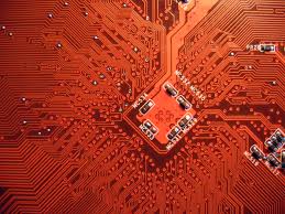 A printed circuit board,
or PCB, is used to mechanically support and electrically connect electronic components
using conductive pathways,
tracks or signal traces etched from copper
sheets laminated onto a non-conductive substrate. It is also
referred to as printed wiring board (PWB) or etched wiring
board. Printed circuit boards are used in virtually all but the simplest
commercially produced electronic devices.
A printed circuit board,
or PCB, is used to mechanically support and electrically connect electronic components
using conductive pathways,
tracks or signal traces etched from copper
sheets laminated onto a non-conductive substrate. It is also
referred to as printed wiring board (PWB) or etched wiring
board. Printed circuit boards are used in virtually all but the simplest
commercially produced electronic devices.
A PCB populated with
electronic components is called a printed circuit assembly (PCA),
printed circuit board assembly or PCB Assembly (PCBA). In
informal use the term "PCB" is used both for bare and assembled
boards, the context clarifying the meaning.
Alternatives to PCBs include wire wrap and point-to-point construction.
PCBs must initially be designed and laid out, but become cheaper, faster to
make, and potentially more reliable for high-volume production since production and soldering of PCBs
can be automated. Much of the electronics industry's PCB design, assembly, and
quality control needs are set by standards published by the IPC organization.
Event Details:
Date:4th October 2012
For more details contact:
Abhishek Mahajan
Mobil Number:9503279884
